Dom
Ronnie say that primary and L2 on one core , and secondary and L1 on the other. Or I miss something?
Ronnie say that primary and L2 on one core , and secondary and L1 on the other. Or I miss something?
U60x55x15-CF138-web2.jpg)
Why Ronnie dont answer. He is our teacher.
The biggest problem with finding a core is finding one with the right characteristics....If the AL is too high getting the right inductance values will result in too much loss of coupling.
That's why Stan used a core with such a small area.
Here are my coils i have removed them from my housing as the secondary coil is splitting and needs to be replaced.
The second pic is how i have wired it.
"small changes and we are good to go..." ~Russ
Lately Matt and others have discovered that Stan's Drive circuit changes the duty cycle as the frequency changes, mine does not do that.
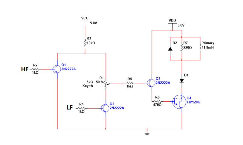
I've been asked about my drive circuit. So here it is. You will likely have to change some of the resistor values to get it working correctly. I just drew it up without checking the values in my circuit as I've made so many changes to it over the last few weeks. It drives the coil just fine but no resonance so no guarantees it will work.
Lately Matt and others have discovered that Stan's Drive circuit changes the duty cycle as the frequency changes, mine does not do that.
The work continues, now you guys know how to get variable amplitude pulsing during the off time though!
Also, if you want to add a DC bias simply connect a pot from Vdd to gnd then put the center pin on the base of the Tip120, that's what I'm doing, using a 5k pot with a 1K resistor at the Tip120 base.
Webmug,
I use a dual channel frequency gen....First I put the Hf and Gate through a 4011 and 4013 ic to sync the two then combine them two using a few 2n2222's which drive the base of a TIP120.
It's all on a breadboard right now so I don't have a schematic yet....I'm waiting on a smaller value pot because the TIP120 is not switching the lower amplitude pulses. Still refining things a bit, but so far I get clean square waves to the TIP120 base unless I take the voltage too high.
Adys15,
I use a dual channel signal gen to produce the high and low frequency pulsing. The +10V supply rail first goes through a 10k resistor, the circuit then splits, one leg goes to the collector of a 2n2222 which base is driven by the high frequency signal. The other leg off the 10k resistor goes through a pot then to the collector of another 2n2222 that is driven by the low frequency signal. The pot controls the pulse amplitude during the "off time".
The center post of the pot drives the base of another 2n2222 which drives the base of the TIP120.
I'll draw up a basic schematic later if you need, just let me know. Right now it's all on a breadboard.
Doesn't matter Russ. Scope through the driver circuit and you will see the 50% duty cycle is maintained all the way through until you get to the base of the TIP120--that's where you'll see duty cycle gets altered.
Matt, I checked the base of the TIP120 in my circuit, I don't see any change in duty cycle as I increase the frequency?
Are you sure it's not part of the voltage amplitude control circuit?
Positive.
Build the VIC circuit as we have posted in this thread and scope through each transistor. Until you get to the TIP120, you will see a nice 50% duty cycle. At that final drive is where you'll see the voltage shift that causes the TIP120 to lag at turn-off. As you up the frequency, you'll get to a point where the output of the TIP120 is always on--100% duty cycle. To me this behavior looks clearly by design. It's a linear tapering of the duty cycle controlled by the frequency. What that means is you can precisely control the duty cycle to PPM resolution by adjusting the frequency. And as I mentioned before, my theory is the off-time should sync with the L2 and the on-time with the L1--the L2 being slightly higher frequency (shorter wire length). I honestly think the wire length on those two chokes is far more important than anyone has considered to this point. They control the exact phasing the cell sees. Brettly posted some wavelength numbers in the centimeter range that is critical to water disassociation. So we're talking phase shift frequencies in the gigahertz range.
